TSMC Bets on Unorthodox Optical Chips for AI data centers
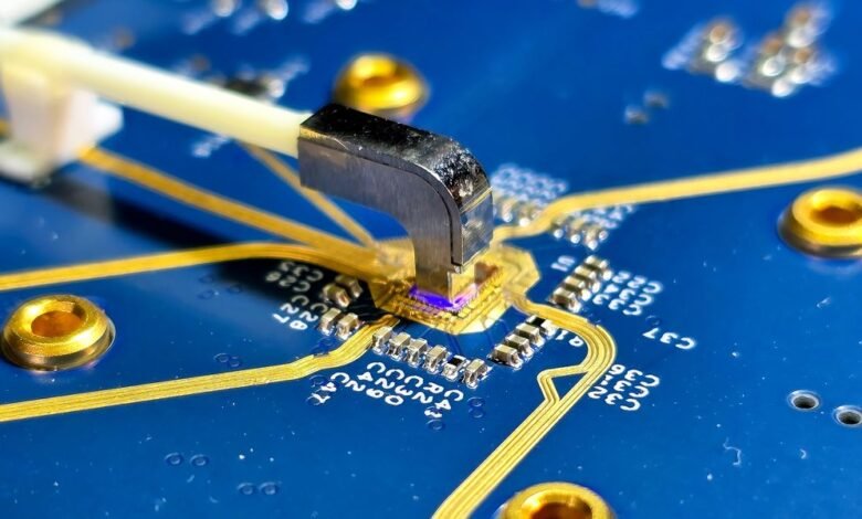
In the race to Everyone Artificial Intelligence Data Center, a main player has now placed a bet on a different horse. Glossary -semiconductor manufacturer Taiwan semiconductor (TSMC has been announced It will work with Sunnyvale startup Aveccina To produce micro -based bonding. This technology is a practical development on replacing electrical communications with visual effects to meet the high needs of communication between an increasing number of graphics processing units in a low -cost and effective energy.
Thanks to the mathematical requirements for large language models and their cousins, artificial intelligence groups face unprecedented requirements regarding data amounts, domain display, cumin and speed. Soon or later, the copper wires that connect the processors and memory within the AI data center rack should be one Replace optics. “There is a big boost to get visual communications as soon as possible,” says Lucas Tsai, TSMC vice president.
Avicena offers a unique approach, using hundreds of blue Micros connected to the type fiber to transfer data. Company units Lightbundle platform It avoids laser problems and associated complexity, which threatens reliability, cost and energy consumption from other visual numbers. “He is very unconventional,” says Tsai. But this is perfect for short distance applications, which is exactly what makes them interesting.
Laser -free
Today’s visual communications carry huge amounts of dozens of data to hundreds of meters through data centers at very high data rates. Traditionally, the usible stereotype connects optical fibers to the rift, as it turns between electrical and visual signals. Companies are making steps to get rid of the transmission and reception devices that can be assembled in the field of energy using packed optics (CPO), which instead leads to visual electrical transformations adjacent to the silicone segment itself. Commercial versions are present Network keyAnd the initial models take steps Towards the graphics processing unit. The most prominent visual optical designs are coded on electronic tattoos on multiple wavelengths of light using the laser and the bound.
However, the main challenge of laser -based visual interconnection is the laser itself. Laser and fiber attachments caused the biggest problems in terms of reliability, manufacturing and cost. Moreover, one optical fiber that hosts dozens of GPU-To-BUCH links in the form of multiple wavelengths suffer from general mathematical expenses: it is much simpler that each lane will transfer data on a separate material channel instead of analyzing one large channel at a later time.
This is the place Avicena comes. Instead of sending a multi-length wavelength below the optical fibers and then analyzed it in individual channels, the interconnected Lightbundle connects hundreds of blue Microeds to a scout of a scout by multiple imaging fibers-and one per 10GB in the second data corridor. The transmission device works like a miniature display and detector like the camera. “We are conducting visual interconnection without the complication of the laser,” says Bardia Pizchki, CEO of Avisina.
A simple visual association can extend with only 300 pixels at 10 GB/s per lane at a distance of 10 meters, which carries the total net 3 terabits per second. Since offers and cameras can expand to millions of pixels, technology can expand to much higher data rates in much lower energy and a much higher density than copper wires.
Mature industry
One of the main features that Avicena described is that its technique mocked LEDS, cameras and shows: all mature industries. “We can expand the scope of our approach to folders and costs that require much more quickly than if we were developing new building blocks,” says Pezeshki. Although silicon has a 30 -year start on visual connections, they must develop new ingredients such as ring ringing and combing. “It takes a lot of time to mature these things,” he says. On the contrary, Lightbundle does not require only simple adjustments to current camera and display technologies.
This is one of the main reasons that TSMC has registered to produce the optical detection sects for the visual escalation of Avicena. “LEDS is already a mature industry; there are a lot of consumer products,” says Tsai. Of course, LEDS is less powerful than lasers-but, for example, 10 meters inside and crossed, this is enough. “There is a possibility to be much cheaper, and it has a lot of repetition,” says Tsai.
Avicena results are already “blowing away” what silicon optical optical can do, according to Bezishki. The initial model of light has already shown the use of energy without deciding for the entire link, as other visual methods “to show” 5 PJ/Bit Energy consumption.
Pezeshki admits that Avicena has ways to go to building the product and expanding its scope. But “the combination of showing great results with the use of mature basic building blocks beats the converts.”
From your site articles
Related articles about the web
Don’t miss more hot News like this! Click here to discover the latest in AI news!
2025-05-26 14:00:00